
What Is Nano V-Cut Fabrication Technologies
VCUT, or Vertical-Cavity Surface-Emitting Laser (VCSEL) Ultra-Thin epitaxial layer growth, is a cutting-edge nanomanufacturing technique that holds immense promise for revolutionizing various technological fields, particularly in optics, photonics, and telecommunications.
This innovative approach to nanomanufacturing involves the precise growth of ultra-thin epitaxial layers in vertical-cavity structures, enabling the production of high-performance VCSEL devices with enhanced efficiency, reliability, and functionality.
Nano V-Cut Fabrication Manufacturer In China
As industries continue to miniaturize their products due to demand for ever smaller and more efficient technologies, the need for tighter tolerance machining and manufacturing processed continues to grow. It is not uncommon to see various components be manufactured at BE-CU Nano Manufacturing Solutions that are not visible to the naked eye. The extremely high magnification automated V-Cut systems produced by our micro manufacturing group are directly integrated into the nano machining operations and processes used by the Micro machining department at BE-CU to machine impossibly small and delicate parts while meeting tolerances as tight as 1 micron.
Our V-Cut equipment is utilized for ultra-precision machining in display optics and illumination optics, enabling nano-precision cutting of non-metals or metals such as copper, nickel, and mold steels with HRC60 or below directly.
- It can directly cut mold steels with hardness below HRC60 without the need for nickel plating, effectively reducing processing cycles.
- Various microstructure teeth can be directly cut. Effective stroke 60um
- Excellent reproducibility with roughness less than Ra0.008, resulting in easier handling of lamp front effects and improved brightness.
- Advanced one-key VCUT with built-in programming capability, no additional programming or learning of G-codes required.
- Fully constrained natural granite air static pressure guide rails, providing excellent long-term machine stability.
- The W-axis is PZT-driven and includes vibration knife function, capable of processing composite microstructure VCUT.
- Air-floating platform base prevents machining errors caused by external vibrations.
Contact us to learn more about micro prototype and bulk nano manufacturing and how they can benefit your business. We’ll also be happy to provide a no-obligation price quote for any of our micromanufacturing services.
Advantages Nano V-Cut Fabrication
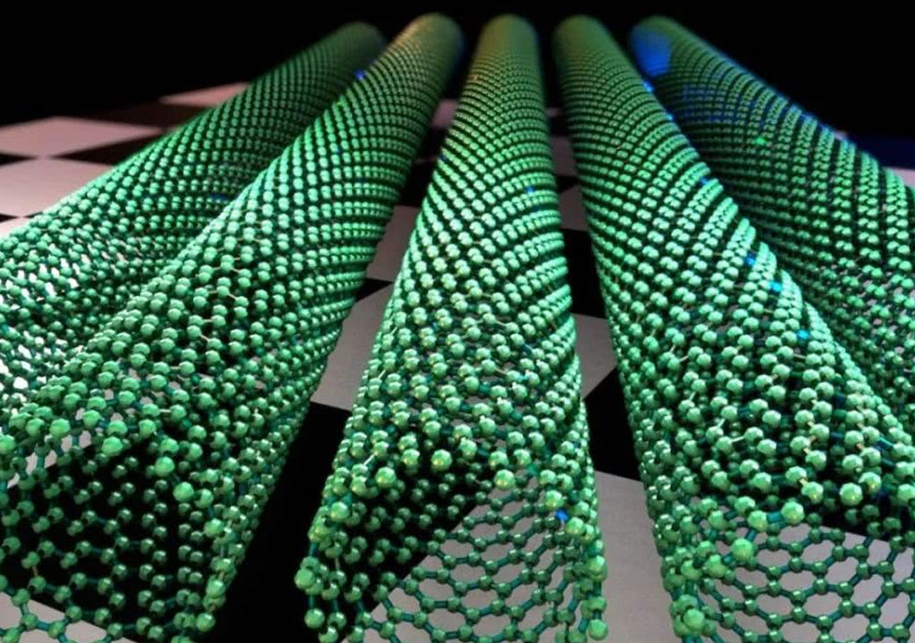
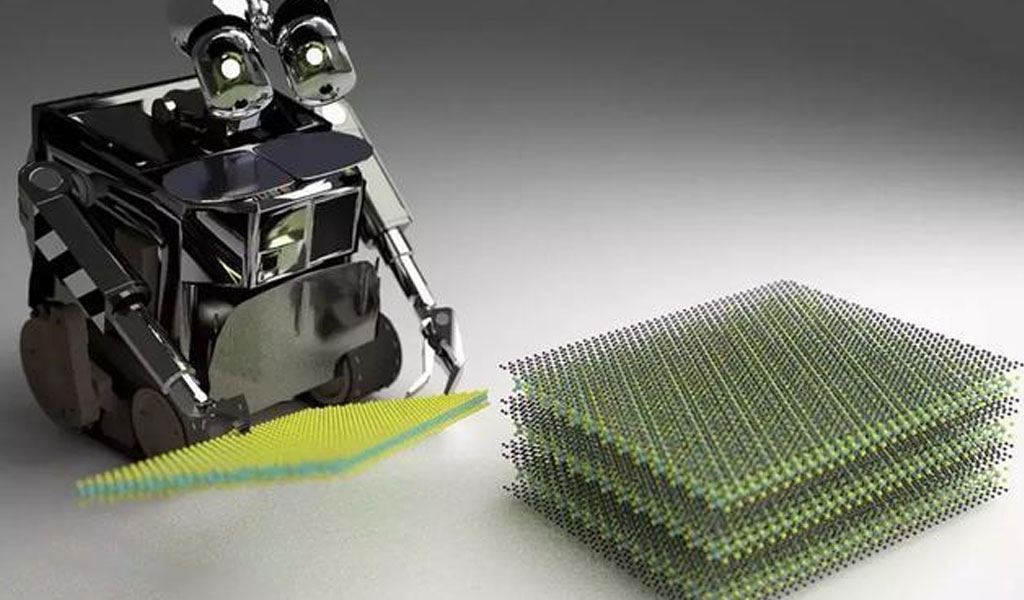
VCUT nanomanufacturing relies on molecular beam epitaxy (MBE) or metalorganic vapor phase epitaxy (MOVPE) techniques to deposit atomically precise layers of semiconductor materials on a substrate. Unlike traditional growth methods, which typically involve lateral expansion, VCUT focuses on vertical growth within confined cavities or wells. This vertical growth approach allows for the fabrication of ultra-thin layers with exceptional uniformity and control over thickness, composition, and crystal quality.
- VCUT enables the fabrication of VCSEL devices with ultra-thin active layers, resulting in reduced optical losses, faster modulation speeds, and improved efficiency. The precise control over layer thickness and composition enhances the optical properties of the devices, leading to superior performance characteristics such as higher output power and lower threshold currents.
- Miniaturization: By reducing the thickness of epitaxial layers, VCUT facilitates the miniaturization of VCSEL devices, making them ideal for compact, high-density optical interconnects and sensor applications. The smaller footprint and lower power consumption of VCUT-produced VCSELs contribute to the development of next-generation optoelectronic systems for data communication, sensing, and imaging.
- Reliability: The uniformity and quality of epitaxial layers grown through VCUT result in VCSEL devices with enhanced reliability and long-term stability. The precise control over material properties reduces defects and improves device uniformity, leading to consistent performance over time and under varying operating conditions.
- Versatility: VCUT nanomanufacturing can be applied to a wide range of semiconductor materials, including III-V compound semiconductors such as gallium arsenide (GaAs) and indium phosphide (InP), as well as emerging materials like gallium nitride (GaN) and gallium oxide (Ga2O3). This versatility enables the production of VCSEL devices tailored to specific applications and wavelength ranges, expanding their potential use cases in diverse fields.
The Application Of Nano V-Cut Fabrication
The applications of VCUT nanomanufacturing are vast and span across multiple industries:
- Data Communication: VCSELs produced using VCUT technology are integral components in high-speed optical communication systems, enabling the transmission of data over short distances with minimal latency and energy consumption. They are used in data centers, telecommunications networks, and consumer electronics for applications such as fiber-optic communication, optical interconnects, and 3D sensing.
- Sensing and Imaging: VCSEL-based sensors and laser diode arrays manufactured using VCUT nanomanufacturing offer high-resolution imaging and precise sensing capabilities for applications in automotive LiDAR systems, facial recognition, gesture recognition, and industrial automation. The compact size and low power consumption of VCSELs make them ideal for integration into portable devices and IoT platforms for environmental monitoring, biomedical imaging, and augmented reality applications.
- Biophotonics and Medical Devices:
Our Case Studies Gallery Of Nano V-Cut Fabrication
As our name suggests, prototype and micro manufacturing services are what we are known for. Over the past 30 years, we’ve completed thousands of projects using electrical discharge machining. What differentiates BE-CU micro nano manufacturing solutions manufacturing services from the competition is our ability to not only hold micron tolerances but to do so while still offering globally competitive pricing and lead times. Utilizing our vast knowledge of Nano V-Cut Fabrication techniques and decades of industry experience, we are confident that we can produce your most challenging components to your exact specifications. To learn more about how BE-CU can help you contact our manufacturing team with your request for quote.
Curved-V-CUT-Structure 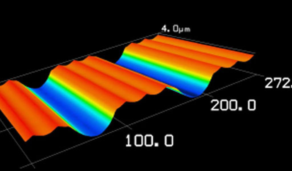
Light-Guide-Plate-Molds-Micro-Groove-Cut 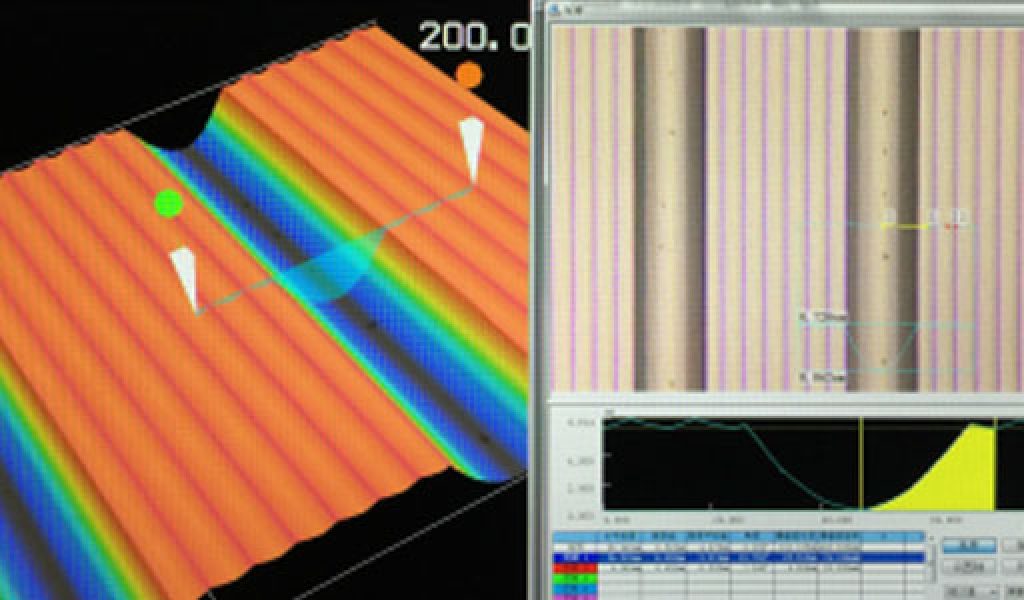
Light-Guide-Plate-Molds-Micro-Groove-Cut 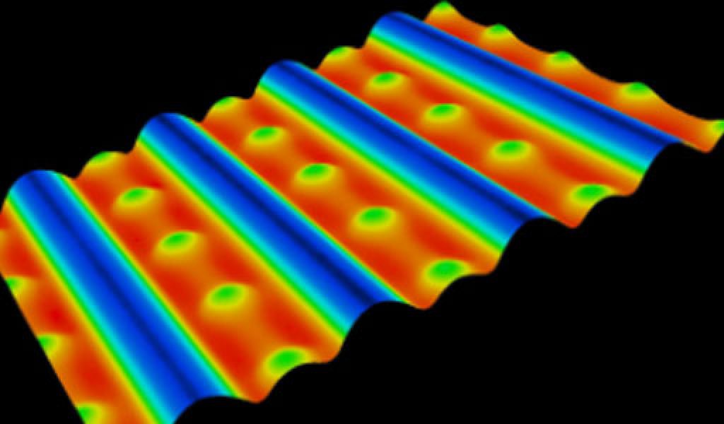
Microstructured-Small-Lens-Depth-0.5um 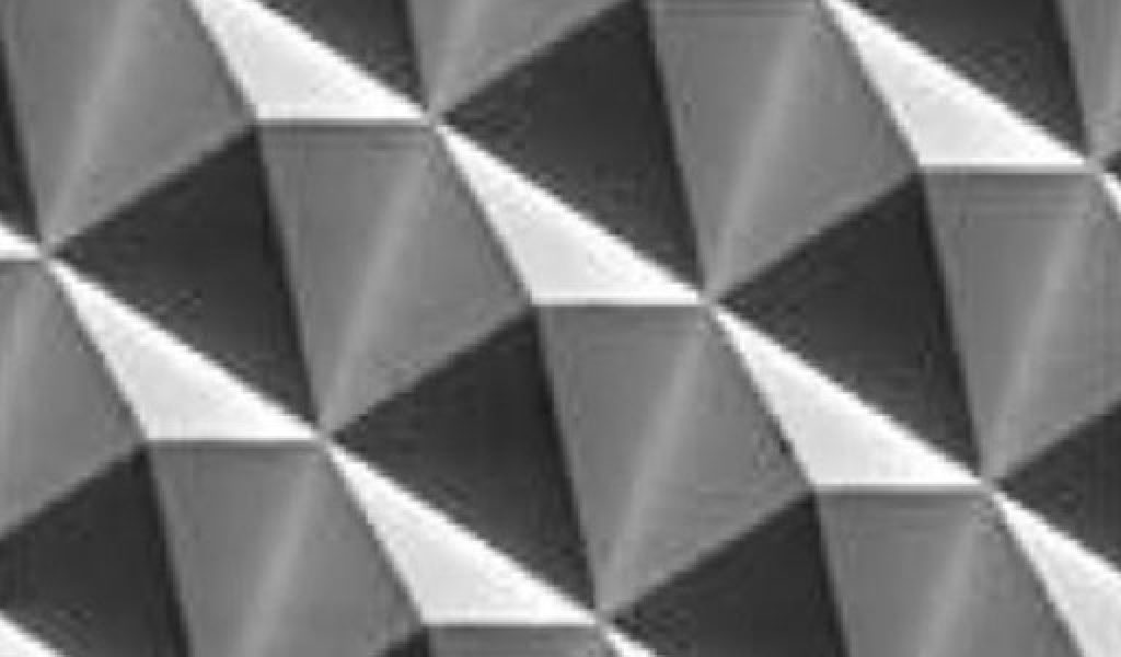
Prism-Die-Fabrication 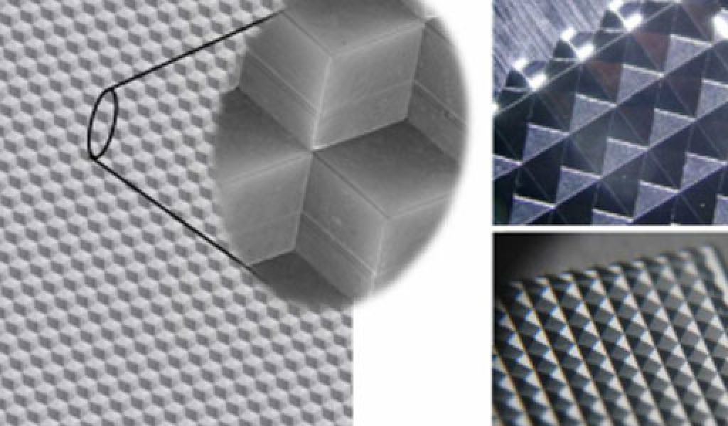
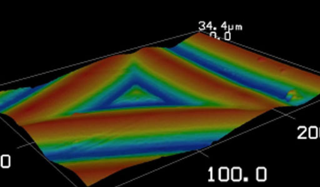
Pyramid-Fabrication 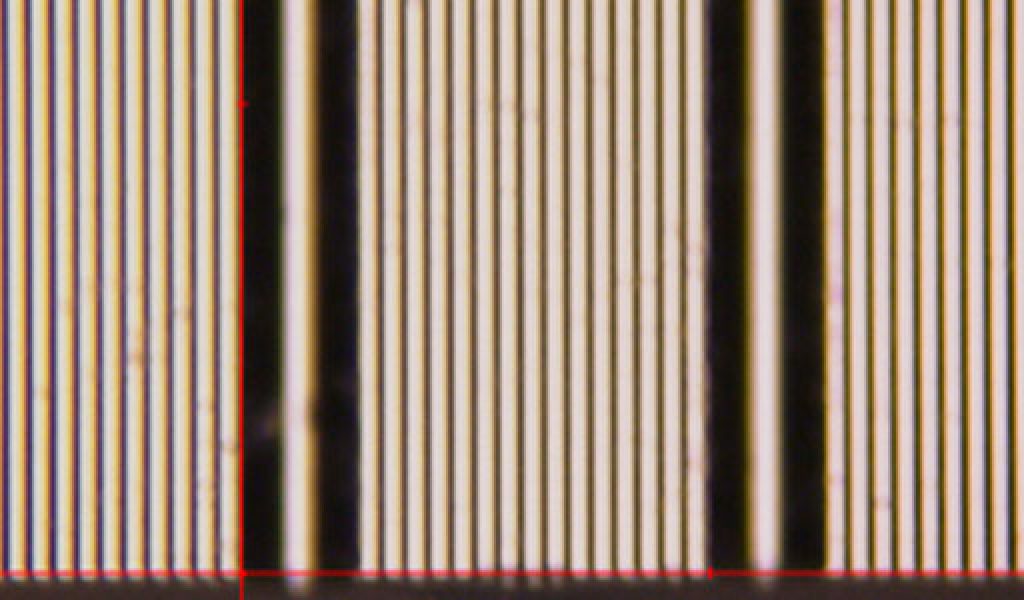
Sawtooth-Die-Tooth-Depth-1.5um 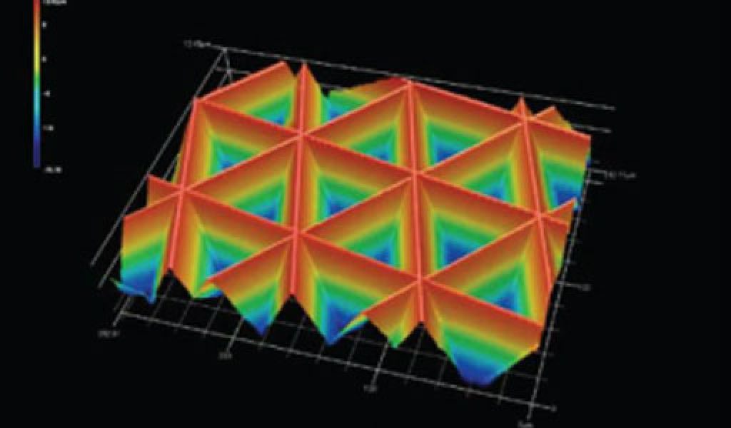
Triangular-pyramid-microstructure-array 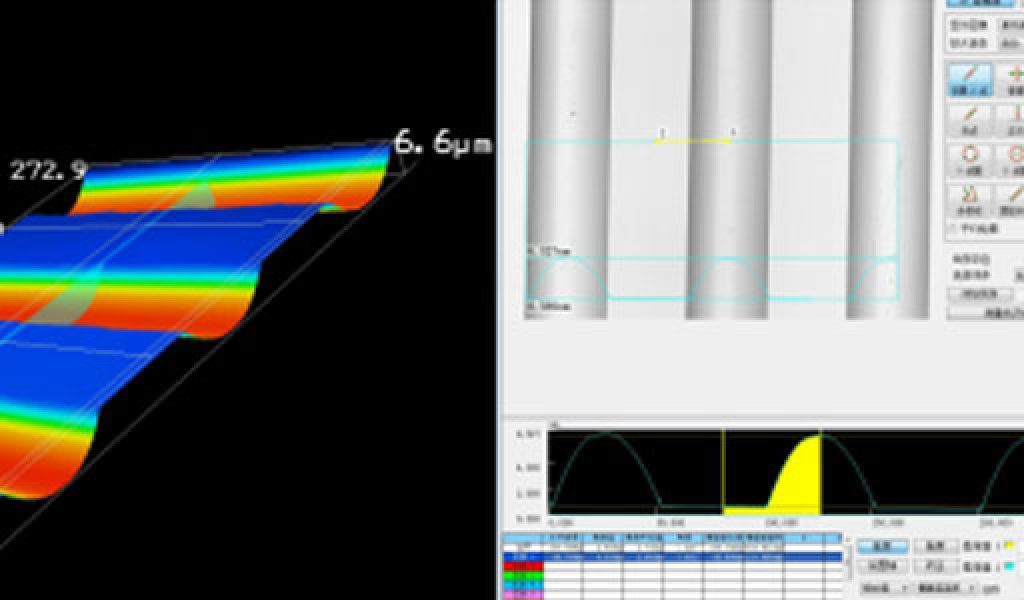
Light-Guide-Plate-Microstructure-Mold-Core