

Microfluidic chips are a cornerstone of modern science and technology, playing an essential role in fields ranging from biology and chemistry to medicine and environmental analysis. These chips, often referred to as lab-on-a-chip (LOC) devices, integrate complex laboratory functions onto a single chip, typically no larger than a credit card. They allow precise manipulation and analysis of small volumes of fluids, enabling a range of applications, from drug discovery to point-of-care diagnostics.The manufacturing of microfluidic chips involves sophisticated techniques that combine elements of chemistry, engineering, and materials science. This article explores the essentials of microfluidic chip manufacturing, including the materials, fabrication processes, challenges, and applications.
Introduction to Microfluidic Chip Manufacturing
Microfluidics involves the control of fluids at the sub-millimeter scale, typically in channels with diameters ranging from tens to hundreds of micrometers. The primary advantage of microfluidic systems is their ability to process tiny amounts of fluid with high precision, which can dramatically reduce the cost and time required for various tests and experiments. The integration of these systems into small, portable devices has further enhanced their utility in various industries.
The manufacturing process for microfluidic chips involves several stages, including the selection of materials, design of microchannels, fabrication of the chip, and testing. The overall goal is to create a device that is both functional and reliable, ensuring that it meets the demands of its intended application.
Materials for Microfluidic Chips
The choice of materials for microfluidic chips is critical, as they directly influence the chip’s performance, durability, and compatibility with various fluids. Several materials are commonly used in the manufacturing of microfluidic devices, each with its own advantages and limitations. These materials are generally classified into polymers, glass, silicon, and metal, with the selection depending on factors such as cost, transparency, chemical resistance, and ease of fabrication.
Polymers
Polymers are among the most commonly used materials for microfluidic chip manufacturing due to their flexibility, ease of processing, and relatively low cost. Common polymers used include:
- Polydimethylsiloxane (PDMS): PDMS is one of the most widely used polymers in microfluidics. It is optically transparent, biocompatible, and easy to mold. PDMS chips can be fabricated using soft lithography, a process that involves creating molds from a patterned master wafer and then casting the polymer into the mold.
- Poly(methyl methacrylate) (PMMA): PMMA, or acrylic, is another polymer used in microfluidics. It offers good optical properties and chemical resistance but is less flexible than PDMS. PMMA chips are often fabricated using laser ablation or hot embossing techniques.
- Cyclic Olefin Copolymer (COC): COC is a transparent polymer with good chemical resistance and thermal stability, making it suitable for applications requiring long-term durability.
- Polycarbonate (PC): Polycarbonate is a strong, transparent material commonly used in the production of microfluidic chips that require high mechanical strength and heat resistance.
Polymers are favored for prototyping due to their low cost and ease of fabrication, but they are often less durable than glass or silicon, particularly in harsh chemical environments.
Glass
Glass is another popular material in microfluidic chip fabrication due to its excellent optical properties, high chemical resistance, and ability to be precisely patterned. Glass microfluidic devices can be fabricated using techniques like photolithography, wet etching, and glass bonding.
- Advantages of glass: Glass microfluidic chips offer high precision and are ideal for applications requiring clear optical analysis, such as fluorescence microscopy. Additionally, glass is chemically inert and can withstand a wide range of solvents, making it suitable for use in analytical chemistry and biomedical research.
- Disadvantages of glass: Glass is relatively brittle, which can lead to breakage during handling. Fabrication of glass microfluidic devices can also be more expensive and time-consuming compared to polymer alternatives.
Silicon
Silicon is a highly versatile material that has been widely used in the fabrication of microelectronics and microelectromechanical systems (MEMS). In microfluidics, silicon is often used in combination with other materials to create complex devices with integrated sensors or actuators.
- Advantages of silicon: Silicon allows for the precise fabrication of microstructures through processes like photolithography and deep reactive ion etching (DRIE). It is also highly durable and can support the integration of electronic components, making it ideal for applications that require both fluid manipulation and electrical functionality.
- Disadvantages of silicon: Silicon is opaque, which limits its use in optical applications. It is also relatively expensive compared to polymers and more difficult to handle due to its rigidity and brittleness.
Metals
Metals such as stainless steel and gold are sometimes used in microfluidic devices, particularly in applications requiring electrical conductivity or heat transfer. Metals are often used in conjunction with other materials, such as in electrodes or fluidic interconnects.
- Advantages of metals: Metals offer excellent conductivity and mechanical strength, making them useful in applications such as electrochemical sensors or microreactors.
- Disadvantages of metals: Metal fabrication can be more challenging than working with polymers or glass, and the cost of high-quality metals can be prohibitive.
Fabrication Techniques for Microfluidic Chips
The fabrication of microfluidic chips requires the precise creation of channels, reservoirs, and other microstructures that control the flow of fluids. There are several key fabrication techniques used in microfluidics, each with its own set of advantages and limitations.
Soft Lithography
Soft lithography is one of the most widely used methods for fabricating microfluidic devices, particularly those made from PDMS. The process involves creating a patterned master wafer, typically from silicon or photomasks, and then casting PDMS onto the wafer to form the microchannels.
- Process steps: The first step is to prepare a master template, which is typically created using photolithography to define the desired pattern on a silicon wafer. The wafer is then coated with a thin layer of photoresist, which is exposed to ultraviolet light through a mask to transfer the pattern. The exposed photoresist is developed, leaving behind a raised pattern. This pattern is then used as a mold for casting the PDMS.
- Advantages: Soft lithography is simple, low-cost, and scalable, making it ideal for prototyping and low-to-medium-volume production. It also allows for the creation of complex, three-dimensional microfluidic structures.
- Disadvantages: The primary limitation of soft lithography is that it is often limited to polymer-based materials like PDMS, which may not be suitable for all applications.
Photolithography
Photolithography is a common technique for creating microstructures on substrates such as glass or silicon. It involves the use of light to transfer a pattern from a photomask onto a photosensitive material, which is then etched to form the desired structure.
- Process steps: A thin layer of photoresist is applied to the substrate, and the substrate is then exposed to ultraviolet light through a photomask. The exposed photoresist is then developed, and the underlying material is etched away to create the microchannels.
- Advantages: Photolithography provides high-resolution patterning and is suitable for creating microstructures on both glass and silicon. It is widely used in both research and commercial microfluidic chip fabrication.
- Disadvantages: Photolithography can be complex and expensive, particularly when working with high-resolution masks or when large volumes of chips are required.
Hot Embossing
Hot embossing is a process in which a patterned mold is pressed into a polymer sheet under heat and pressure to create microfluidic channels. This technique is particularly useful for thermoplastic polymers like PMMA or COC.
- Process steps: A patterned mold is heated to a specific temperature, and pressure is applied to the mold to transfer the pattern onto a polymer sheet. The polymer is then cooled, solidifying the microfluidic channels.
- Advantages: Hot embossing is a relatively simple and cost-effective technique for mass production of microfluidic chips. It allows for the use of a wide range of thermoplastic materials.
- Disadvantages: The resolution of the process may be limited by the quality of the mold, and some materials may require higher temperatures or specialized equipment.
Laser Ablation
Laser ablation is a process used to etch or ablate microchannels into polymer substrates. This technique uses a focused laser beam to vaporize material, creating precise features on the surface of the chip.
- Process steps: A laser is focused onto the surface of a polymer sheet, where it is used to ablate material in the desired pattern. The laser’s intensity and focal length can be adjusted to control the depth and width of the ablation.
- Advantages: Laser ablation is a highly precise method that can be used to create microfluidic features in a variety of materials. It also allows for rapid prototyping and small-scale production.
- Disadvantages: Laser ablation may not be suitable for all materials, and the process can be slow for large-scale production.
Bonding Techniques
Once the microfluidic channels are created, the chip needs to be sealed to prevent leakage. Bonding techniques are essential for this step, and several methods are commonly used in microfluidics:
- Thermal bonding: This involves applying heat and pressure to bond two polymer layers together. It is commonly used for PDMS-based chips.
- UV bonding: This method uses ultraviolet light to cure a layer of adhesive, bonding two substrates together. It is often used for bonding glass or PDMS to other materials.
- Plasma bonding: Plasma treatment is used to activate the surface of a material, making it more adhesive and allowing it to bond with another material under pressure.
- Adhesive bonding: Special adhesives can be used to bond different layers of a microfluidic chip, particularly when working with materials like glass or metal.
Challenges in Microfluidic Chip Manufacturing
Despite its many advantages, microfluidic chip manufacturing faces several challenges that can impact the performance and scalability of these devices.
Scaling Up Production
While techniques like soft lithography and hot embossing are suitable for prototyping, they may not be ideal for large-scale production. Scaling up production requires the development of more efficient fabrication processes that can handle high volumes while maintaining the precision and quality of each chip.
Material Selection
The choice of material is a critical factor in microfluidic chip manufacturing. Each material has its own set of advantages and limitations, and selecting the right material depends on the specific application. For example, PDMS is easy to work with but may not be suitable for long-term use in chemical environments, while glass is more durable but harder to fabricate.
Integration of Components
Microfluidic chips often require the integration of other components, such as sensors, actuators, and pumps. Integrating these components into the chip without compromising its performance or functionality remains a significant challenge.
Fluidic Control
Controlling the flow of fluids through microchannels can be challenging, particularly when working with complex fluids or when precise control is required. Developing systems that can regulate flow rates, pressures, and mixing conditions is crucial for the success of many microfluidic applications.
Applications of Microfluidic Chips
Microfluidic chips have a wide range of applications, particularly in the fields of biology, medicine, chemistry, and environmental science. Some of the most prominent applications include:
- Point-of-care diagnostics: Microfluidic chips are used in portable diagnostic devices that can quickly analyze blood, urine, or other fluids, enabling rapid detection of diseases or infections.
- Drug discovery and development: Microfluidics is used to model biological systems and screen potential drug candidates more efficiently than traditional methods.
- Environmental monitoring: Microfluidic chips can be used to detect pollutants in water or air, providing real-time data for environmental monitoring.
- Synthetic biology: Microfluidics allows researchers to manipulate biological systems at the cellular level, facilitating the development of new synthetic biology applications.
- Chemical analysis: Microfluidic devices are used for precise chemical reactions, mixing, and analysis, allowing for miniaturized and more efficient chemical processing.
Conclusion
Microfluidic chip manufacturing is a dynamic and rapidly evolving field that combines multiple disciplines, including materials science, engineering, and chemistry. The development of microfluidic devices has revolutionized many industries by enabling more efficient, cost-effective, and precise fluid handling. Although challenges remain, advancements in fabrication techniques and materials are driving the growth of this field, ensuring its continued impact on science, medicine, and industry for years to come.
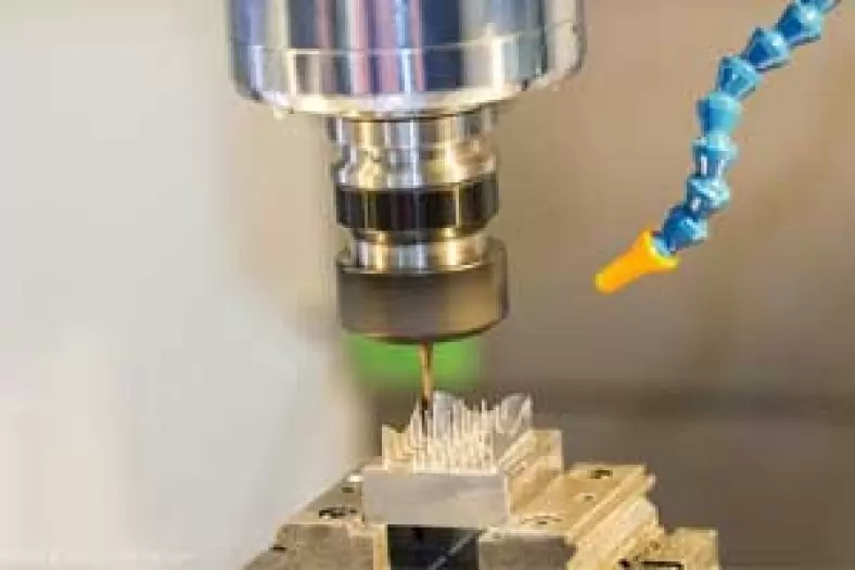
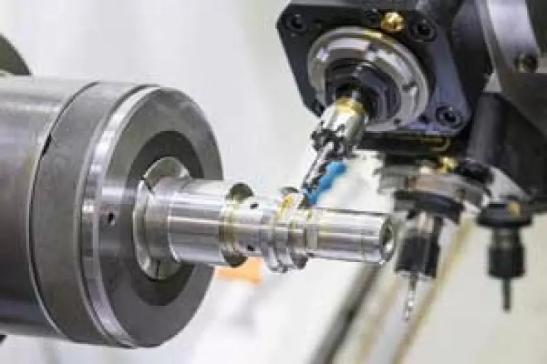
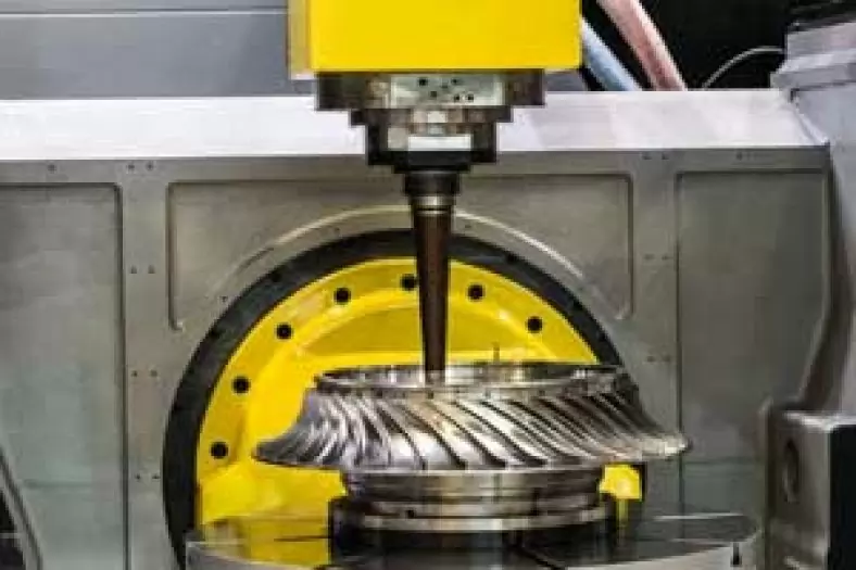
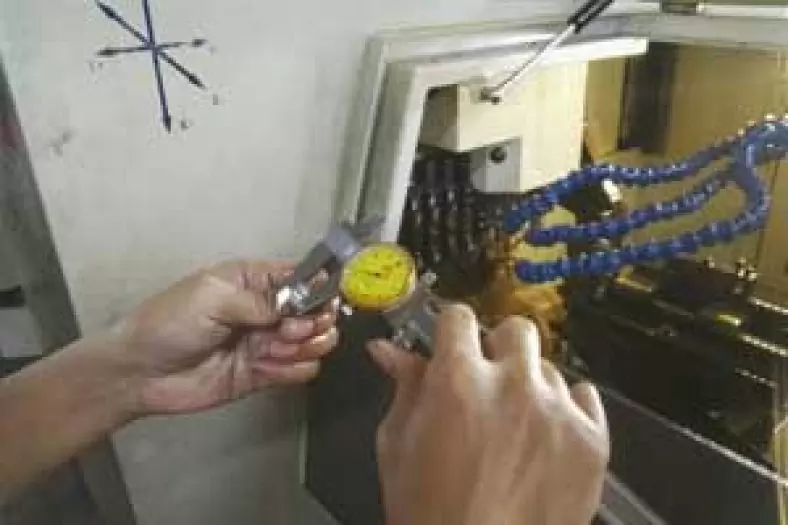
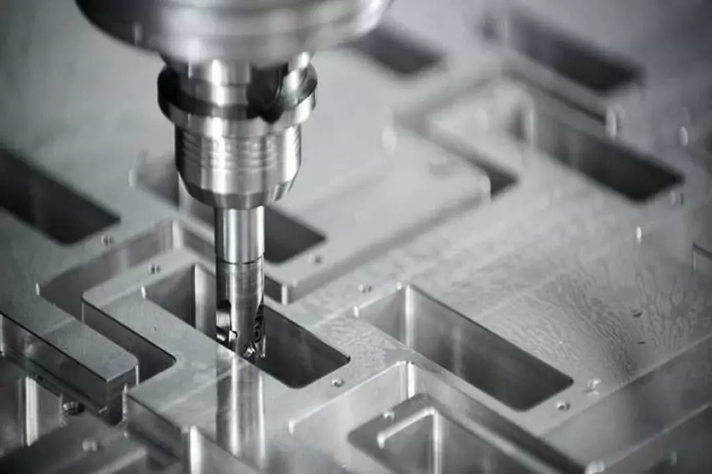
The Detail Of BE-CU Cnc Machining Shop
BE-CU.COM – As an accomplished CNC machining Service Manufacturer and CNC shop, BE-CU Prototype has been specialized in OEM CNC lathing, custom CNC machining parts production and rapid CNC machining services China for over 35 years and always maintaining the highest standard in delivery speed and reliable quality of precision CNC manufacturing components. With the help of high-level technology and efficient equipment, as well as rigorous attitude, BE-CU passed the ISO9001:2015 quality certification, which supports the long-term development of CNC milling services, CNC turning services, CNC milling-turning, CNC drilling services, 3/4/5 axis machining, gear machining services, CNC machining China custom parts and service, small parts machining, etc.Our CNC machining products can be utilized in a broad range of industries. Contact us for email: [email protected]
-
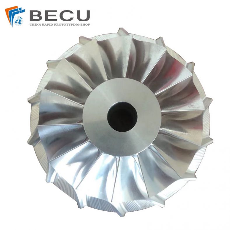
3-Way Centrifugal Compressor Closed Impeller By 5 Axis Machining
-
3/4/5 Axis Precision Milling Custom Vehicle Parts
-
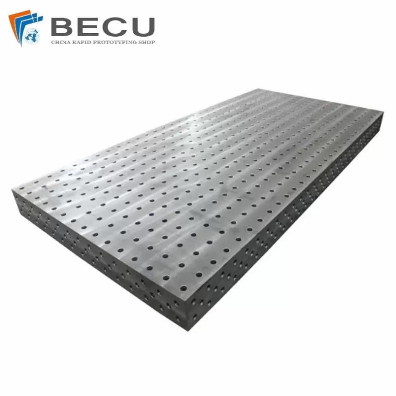
3D Flexible Welding Platform By Large Machining
-
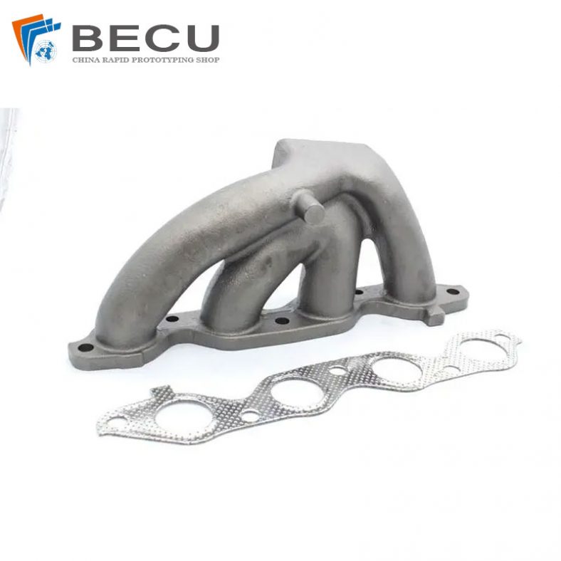
3D Printed Inconel Exhaust Manifold
-
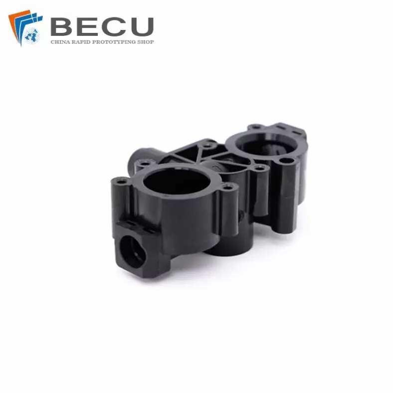
3D Printing And CNC Machining Custom Black PPS Valve
-
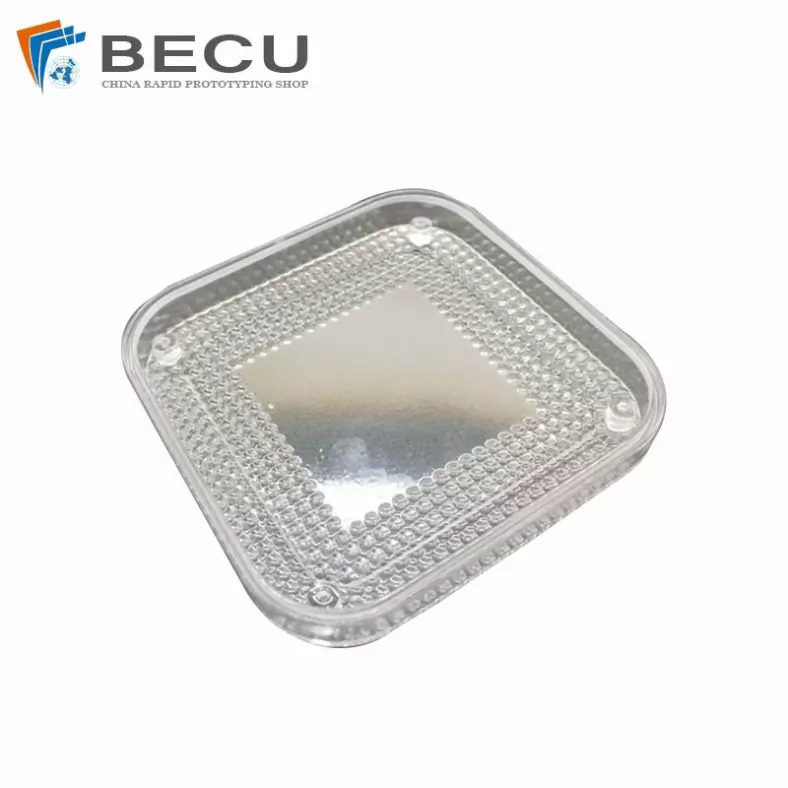
3D Printing Full Transparent Acrylic Lampshade Model
-
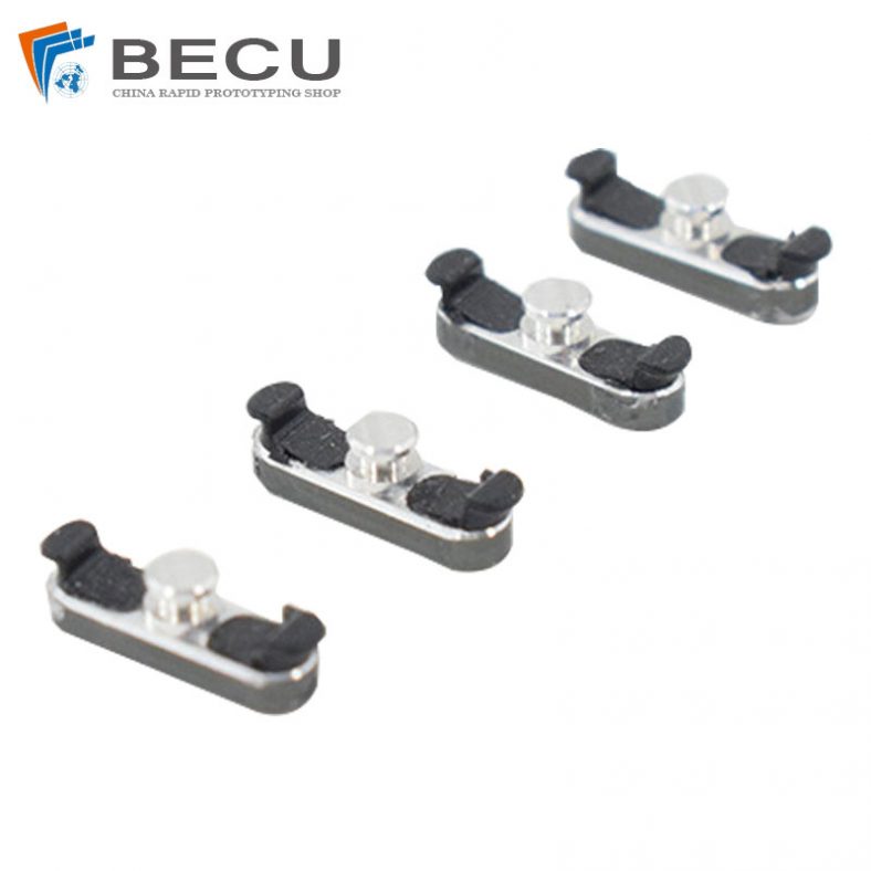
4 Axis CNC Machining Titanium Grade 5 Mobile Phone Buttons
-
4 Axis Machining Highly Transparent Acrylic LED Tunnel Light Lens