Etching is a fundamental process in microfabrication, widely utilized in the production of integrated circuits (ICs), microelectromechanical systems (MEMS), and other nanoscale devices. It involves the selective removal of material from a substrate, typically a semiconductor wafer such as silicon, to create intricate patterns that define the functionality of the final device.
The two primary etching techniques employed in modern manufacturing are dry etching and wet etching. These methods differ significantly in their mechanisms, precision, applications, and limitations, making them suited to distinct roles within the fabrication process.
This article provides an in-depth exploration of dry etching and wet etching, comparing their differences and detailing their applications across various industries.
Metal-etch.com
Etching processes trace their origins to early material removal techniques, but their modern forms emerged with the advent of the semiconductor industry in the mid-20th century. Wet etching, one of the earliest methods, relies on liquid chemical reactions, while dry etching, a more recent development, leverages gaseous reactants or plasma-based systems. Both techniques have evolved considerably, driven by the demand for smaller, more efficient, and more complex electronic components. Understanding the distinctions between dry and wet etching is critical for engineers and researchers tasked with selecting the appropriate method for a given application.
Fundamentals of Wet Etching
Wet etching is a chemical process that removes material from a substrate through the application of liquid etchants. These etchants, typically acids, bases, or other reactive solutions, interact with the substrate surface, dissolving the exposed material in a controlled manner. The process is isotropic in most cases, meaning it etches uniformly in all directions, resulting in rounded or undercut features beneath a masking layer. This isotropy arises because wet etching depends on the diffusion of chemical species to and from the surface, which lacks directional control.
The wet etching process begins with the preparation of the substrate, often a silicon wafer, coated with a thin film of material to be etched, such as silicon dioxide (SiO₂) or aluminum. A photoresist mask is applied and patterned using photolithography to expose specific regions of the substrate. The wafer is then immersed in or sprayed with the etchant solution, which selectively removes the unprotected material. Common etchants include hydrofluoric acid (HF) for silicon dioxide, phosphoric acid (H₃PO₄) for aluminum, and potassium hydroxide (KOH) for silicon. The reaction products are typically soluble compounds that dissolve into the liquid medium, leaving behind the desired pattern.
Wet etching is valued for its simplicity, low cost, and high selectivity. Selectivity refers to the ability of an etchant to remove one material while leaving another intact, a critical factor when etching multilayered structures. For example, HF etches SiO₂ rapidly but has minimal effect on silicon, making it ideal for certain applications. However, the isotropic nature of wet etching limits its use in modern microfabrication, where anisotropic (directional) etching is often required to achieve high-aspect-ratio features.
Fundamentals of Dry Etching
Dry etching, in contrast, employs gaseous etchants or plasma to remove material from a substrate. Introduced later than wet etching, it has become the dominant technique in advanced semiconductor manufacturing due to its ability to produce anisotropic profiles and finer features. Dry etching encompasses several methods, including reactive ion etching (RIE), plasma etching, and ion beam etching, each with unique mechanisms and applications.
In dry etching, the substrate is placed in a vacuum chamber where a plasma—a partially ionized gas containing ions, electrons, and neutral species—is generated. The plasma is created by applying radiofrequency (RF) or microwave energy to a gas mixture, such as carbon tetrafluoride (CF₄) or sulfur hexafluoride (SF₆). The reactive species in the plasma, such as fluorine radicals, chemically react with the substrate material, forming volatile compounds that are pumped out of the chamber. Simultaneously, energetic ions may bombard the surface, enhancing the etching process through physical sputtering or aiding in the removal of reaction byproducts.
The anisotropy of dry etching stems from the directional nature of ion bombardment, which etches predominantly in the vertical direction. This allows for the creation of steep sidewalls and high-aspect-ratio structures, essential for modern devices with feature sizes in the nanometer range. Dry etching also offers greater control over the etching process through parameters such as gas composition, pressure, and power, enabling precise tailoring of etch profiles.
Chemical and Physical Mechanisms
Wet Etching Mechanisms
The chemical mechanism of wet etching is straightforward: the etchant reacts with the substrate material to form soluble products. For instance, when etching silicon dioxide with HF, the reaction proceeds as follows:
SiO2+6HF→H2SiF6+2H2O
The resulting hexafluorosilicic acid (H₂SiF₆) dissolves in the aqueous solution, leaving the silicon substrate intact if masked. The reaction rate depends on factors such as etchant concentration, temperature, and the crystallographic orientation of the substrate. For anisotropic wet etching of silicon, etchants like KOH exploit the differing etch rates of silicon’s crystal planes (e.g., <100> vs. <111>), producing V-shaped grooves or pyramidal structures.
The isotropic nature of most wet etching processes arises from the diffusion-limited transport of reactants and products. As the etchant penetrates beneath the mask, it etches laterally as well as vertically, leading to undercutting. This limits the minimum feature size achievable with wet etching, typically to the micrometer range.
Dry Etching Mechanisms
Dry etching combines chemical and physical mechanisms, depending on the specific technique. In plasma etching, reactive species chemically attack the substrate. For example, CF₄ plasma generates fluorine radicals that react with silicon:
Si+4F→SiF4
The volatile silicon tetrafluoride (SiF₄) is then evacuated, completing the etch. In reactive ion etching (RIE), ion bombardment enhances this chemical process by providing energy to break surface bonds or remove non-volatile byproducts, increasing etch anisotropy.
Physical etching, such as ion milling, relies solely on the kinetic energy of ions (e.g., argon ions) to sputter material from the surface. While highly anisotropic, it lacks selectivity, as it removes all exposed materials indiscriminately. Most modern dry etching processes, like deep reactive ion etching (DRIE), balance chemical reactivity and physical bombardment to achieve both selectivity and anisotropy.
Process Parameters and Control
Wet Etching Parameters
Wet etching is governed by parameters such as etchant composition, temperature, and immersion time. For instance, increasing the HF concentration accelerates SiO₂ etching but may reduce selectivity to underlying layers. Temperature also plays a critical role; higher temperatures typically increase etch rates but can compromise uniformity if not carefully controlled. Agitation of the etchant solution, through stirring or spraying, enhances uniformity by reducing diffusion limitations.
Mask integrity is another key factor. The photoresist or hard mask (e.g., silicon nitride) must withstand the etchant without degrading, as any breach can lead to unintended etching. Wet etching’s simplicity eliminates the need for complex equipment, requiring only a chemical bath and basic safety measures like fume hoods.
Dry Etching Parameters
Dry etching offers finer control through a broader range of parameters, including gas flow rates, chamber pressure, RF power, and substrate temperature. For example, in RIE, higher RF power increases ion energy, enhancing anisotropy but potentially reducing selectivity. Gas mixtures can be tailored—adding oxygen to CF₄ improves SiO₂ etching by forming additional reactive species, while chlorine-based gases like Cl₂ are used for aluminum etching.
The vacuum environment and plasma generation require sophisticated equipment, such as plasma reactors with precise pressure and power controls. Process monitoring, often via optical emission spectroscopy or mass spectrometry, ensures consistency. However, this complexity increases costs and demands skilled operators.
Advantages and Disadvantages
Advantages of Wet Etching
Wet etching’s primary advantages include its low cost, simplicity, and high throughput. The process requires minimal equipment—a chemical bath and basic cleaning tools—making it accessible for small-scale or less demanding applications. It excels in applications requiring high selectivity, such as removing sacrificial layers in MEMS fabrication. Additionally, wet etching can process multiple wafers simultaneously, enhancing efficiency in batch production.
The technique is also effective for isotropic etching tasks, such as smoothing surfaces or creating rounded features. For example, HF-based wet etching is widely used to polish silicon wafers or remove native oxide layers before further processing.
Disadvantages of Wet Etching
The isotropic nature of wet etching is its most significant limitation, restricting its use in advanced microfabrication where vertical profiles are essential. Undercutting limits feature resolution to several micrometers, far coarser than the nanometer-scale precision required for modern ICs. Wet etching also generates chemical waste, posing environmental and safety challenges. The reliance on liquid handling increases the risk of contamination, and mask adhesion issues can lead to defects.
Advantages of Dry Etching
Dry etching’s key advantage is its anisotropy, enabling the creation of high-aspect-ratio features with near-vertical sidewalls. This precision supports the fabrication of sub-10 nm structures in cutting-edge semiconductor devices. The process is highly controllable, with adjustable parameters allowing engineers to optimize etch rates, selectivity, and uniformity. Dry etching also avoids liquid waste, reducing environmental impact, and is compatible with vacuum-based fabrication workflows.
Techniques like DRIE, which alternates etching and passivation steps (the Bosch process), enable deep, narrow trenches in silicon, critical for MEMS and 3D ICs. Dry etching’s versatility extends to a wide range of materials, including metals, dielectrics, and polymers.
Disadvantages of Dry Etching
Dry etching’s complexity and cost are notable drawbacks. Plasma reactors and vacuum systems are expensive to purchase and maintain, and the process requires skilled personnel to optimize conditions. Selectivity can be lower than in wet etching, especially in physical-dominated methods like sputtering. Additionally, plasma processes may introduce surface damage or contamination, such as ion-induced defects or polymer residues, necessitating post-etch cleaning.
Applications in Industry
Wet Etching Applications
Wet etching remains prevalent in applications where isotropy or high selectivity is advantageous. In silicon wafer preparation, HF is used to remove oxide layers, while KOH etches silicon to create microstructures like diaphragms or cantilevers in MEMS devices. The technique is also employed in solar cell manufacturing to texture silicon surfaces, enhancing light absorption.
In older IC processes, wet etching was standard for patterning metal layers (e.g., aluminum with H₃PO₄) or dielectrics. While largely replaced by dry etching in advanced nodes, it persists in less critical steps or low-cost production lines. Wet etching’s simplicity also makes it a staple in educational labs and prototyping.
Dry Etching Applications
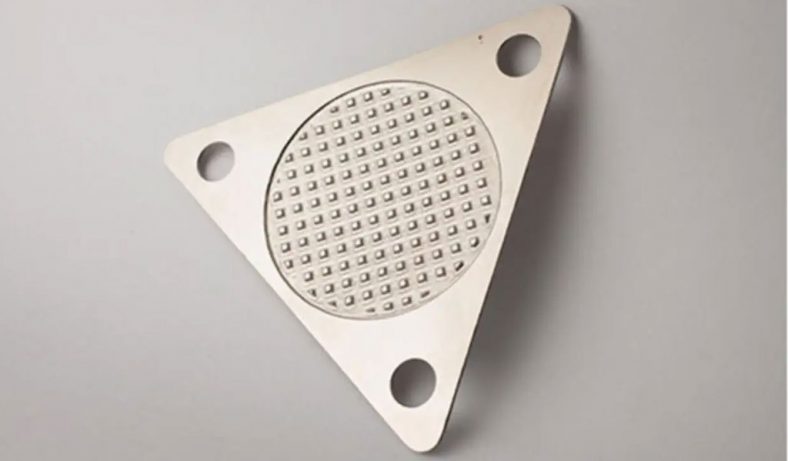
Dry etching dominates modern semiconductor manufacturing, particularly in deep submicron and nanoscale processes. RIE and DRIE are used to define transistor gates, vias, and trenches in ICs, achieving feature sizes below 5 nm. The Bosch process, a DRIE variant, is critical for MEMS, enabling high-aspect-ratio structures like accelerometers and gyroscopes.
In optoelectronics, dry etching patterns waveguides and photonic crystals in materials like silicon or indium phosphide. It is also essential for 3D NAND flash memory, where stacked layers require precise vertical etching. Beyond semiconductors, dry etching processes materials like titanium or sapphire in aerospace and biomedical applications.
Comparative Analysis
Feature Size and Resolution
Wet etching’s isotropic behavior limits its resolution to the micrometer range, typically 1–10 μm, due to undercutting. Dry etching, with its anisotropic control, achieves sub-nanometer precision, critical for advanced nodes like 3 nm in IC manufacturing. This gap reflects their respective roles: wet etching for coarse features, dry etching for fine ones.
Selectivity
Wet etching often exhibits superior selectivity due to its reliance on specific chemical reactions. For instance, HF etches SiO₂ over silicon with ratios exceeding 100:1. Dry etching selectivity varies widely—chemical plasma etching can achieve high ratios (e.g., 50:1 for Si:SiO₂ with SF₆), but physical methods like sputtering are less selective (1:1 or worse).
Equipment and Cost
Wet etching requires minimal investment—chemical baths cost thousands of dollars, compared to millions for dry etching systems like RIE reactors. Operating costs follow suit, with wet etching needing only etchants and waste disposal, while dry etching demands gases, power, and maintenance.
Environmental Impact
Wet etching generates liquid chemical waste, requiring neutralization and disposal, whereas dry etching produces gaseous byproducts, often less hazardous but still requiring scrubbers. Dry etching’s vacuum processes consume more energy, increasing its carbon footprint.
Detailed Comparison Tables
| Parameter | Wet Etching | Dry Etching |
|---|---|---|
| Mechanism | Chemical (liquid reactants) | Chemical (gas/plasma) + Physical |
| Directionality | Isotropic (most cases) | Anisotropic (most cases) |
| Feature Size | >1 μm | <10 nm |
| Selectivity | High (e.g., 100:1 SiO₂:Si) | Variable (e.g., 50:1 Si:SiO₂) |
| Etch Rate | 10–1000 nm/min | 10–500 nm/min |
| Uniformity | Moderate (diffusion-limited) | High (plasma control) |
| Aspect | Wet Etching | Dry Etching |
|---|---|---|
| Primary Equipment | Chemical bath, fume hood | Plasma reactor, vacuum system |
| Initial Cost | $1,000–$10,000 | $500,000–$5,000,000 |
| Operating Cost | Low (etchants, disposal) | High (gases, power, maintenance) |
| Operator Skill | Basic | Advanced |
| Industry | Wet Etching | Dry Etching |
|---|---|---|
| Semiconductors | Oxide removal, metal patterning | Gate/trench etching, 3D NAND |
| MEMS | Sacrificial layers, V-grooves | High-aspect-ratio structures |
| Solar Cells | Surface texturing | Anti-reflective coatings |
| Optoelectronics | Limited use | Waveguides, photonic crystals |
Conclusion
Dry etching and wet etching represent two complementary pillars of microfabrication, each with distinct strengths and weaknesses. Wet etching, with its simplicity and selectivity, remains a cost-effective choice for isotropic tasks and large-scale production. Dry etching, with its anisotropy and precision, is indispensable for the nanoscale features driving modern technology. The choice between them depends on factors such as feature size, material, cost, and environmental considerations, with hybrid approaches offering a potential middle ground.
Wet Etching Innovations
While wet etching has been overshadowed by dry methods in advanced fabrication, research continues to refine its applications. Novel etchants, such as ionic liquids, promise improved selectivity and reduced environmental impact. Techniques like electrochemical wet etching, which applies an electric field to control etch directionality, aim to mitigate isotropy, potentially reviving wet etching’s relevance in niche areas.
Dry Etching Advancements
Dry etching is evolving to meet the demands of next-generation devices. Atomic layer etching (ALE), a plasma-based technique, offers atomic-scale precision by removing material one monolayer at a time. This is critical for 2 nm nodes and beyond, where traditional RIE lacks sufficient control. Additionally, cryogenic dry etching, using low temperatures to enhance selectivity, is gaining traction for materials like gallium nitride (GaN) in power electronics.
Hybrid Approaches
Hybrid etching, combining wet and dry techniques, is an emerging trend. For example, a dry etch may define fine features, followed by a wet etch to smooth surfaces or remove residues. Such approaches leverage the strengths of both methods, optimizing cost, precision, and throughput.
As microfabrication advances, both techniques will continue to evolve, adapting to new materials, smaller scales, and sustainability demands. Their interplay underscores the dynamic nature of manufacturing science, where legacy methods and cutting-edge innovations coexist to shape the technologies of tomorrow.
Metal Etching Material
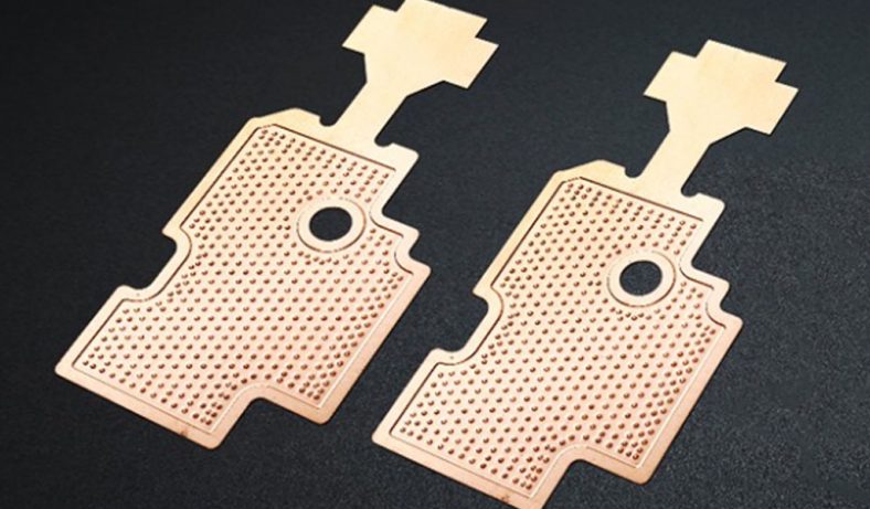

The Detail Of BE-CU Metal Etching Company
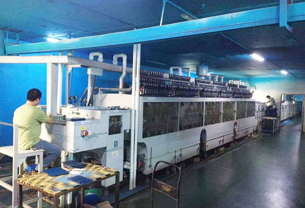
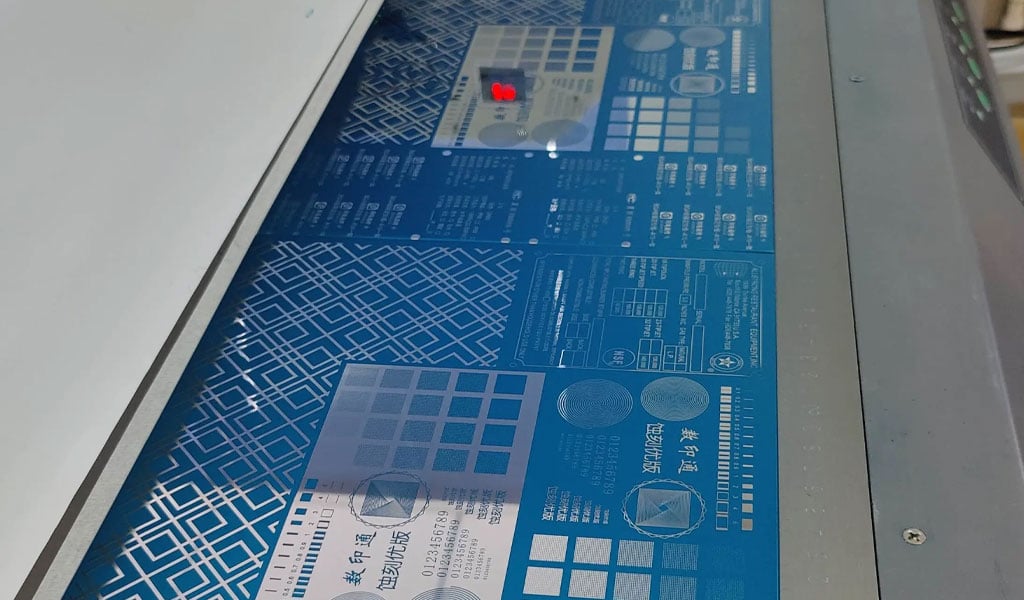
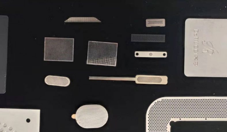
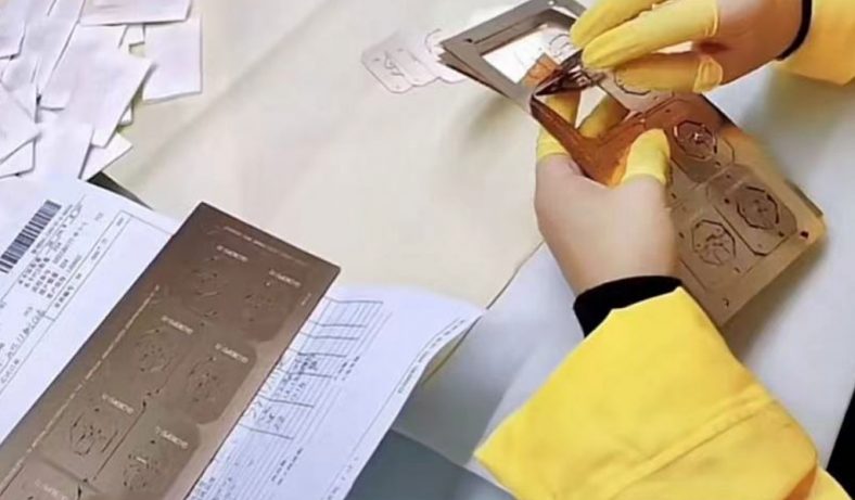
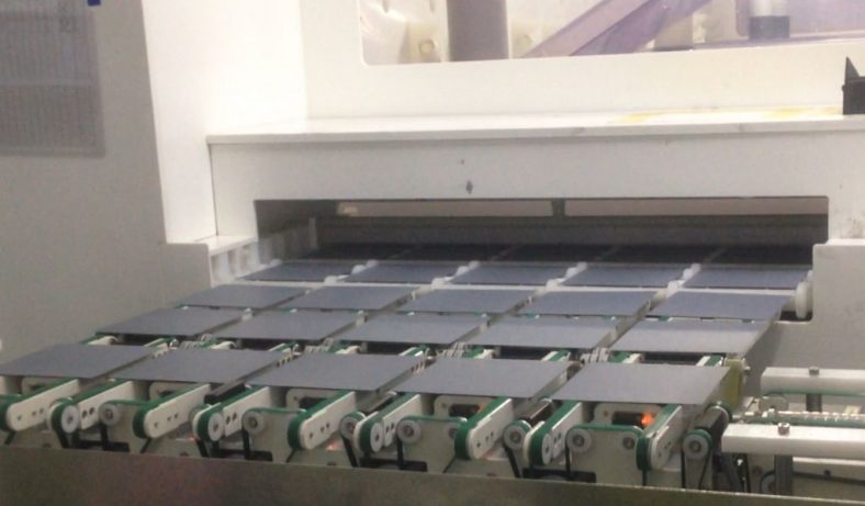
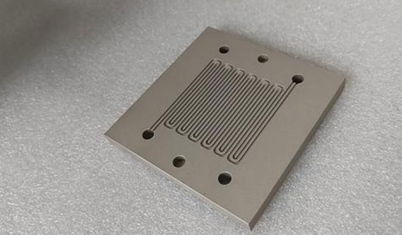
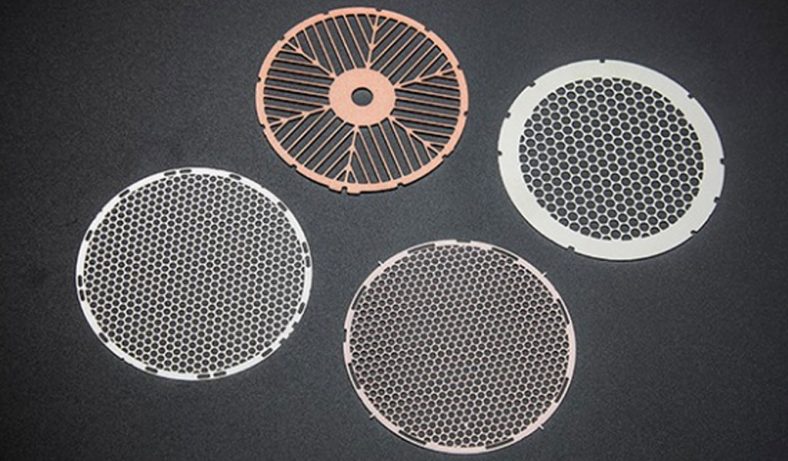
BE-CU Etch has specialized in high precision etchingindustry for over 10 years and supporting globalleading metal etching service in electronics, semiconductor-re-lated, car, new energy sources, and other industrieswith reliable technology and service. Our productsinclude lead frame,IGBT, metal bipolar plate for bat-tery, speaker mesh/interior parts for cars,5G heatsink(VC etching) and high precision metal accesso-ries for notebooks/computer/hardware, etc.
BE-CU precision etching company has passed the certifications of ISO9001/14001,IATF16949,QCO80000, IEC27001.We provide one-stop solutionwith chemical etching, stamping and surface finish, which make us could offer high quality productwith excellent competitive price to our customers and help customers reduce the cost and pressure of supply chain management.